Resources
Find exactly what you're looking for
Enabling the Future of Quantum
Quantum Computing Capabilities

Accelerate Innovation in High-Growth Markets
Quick-turn Manufacturing Capabilities

Strength in Flexibility with High-Velocity Manufacturing
Box Build Capabilities
Strength in Flexibility with High-Velocity Manufacturing
EMS Integration & Test Capabilities
Repatriating PCBA Production
Published in Microwave Journal

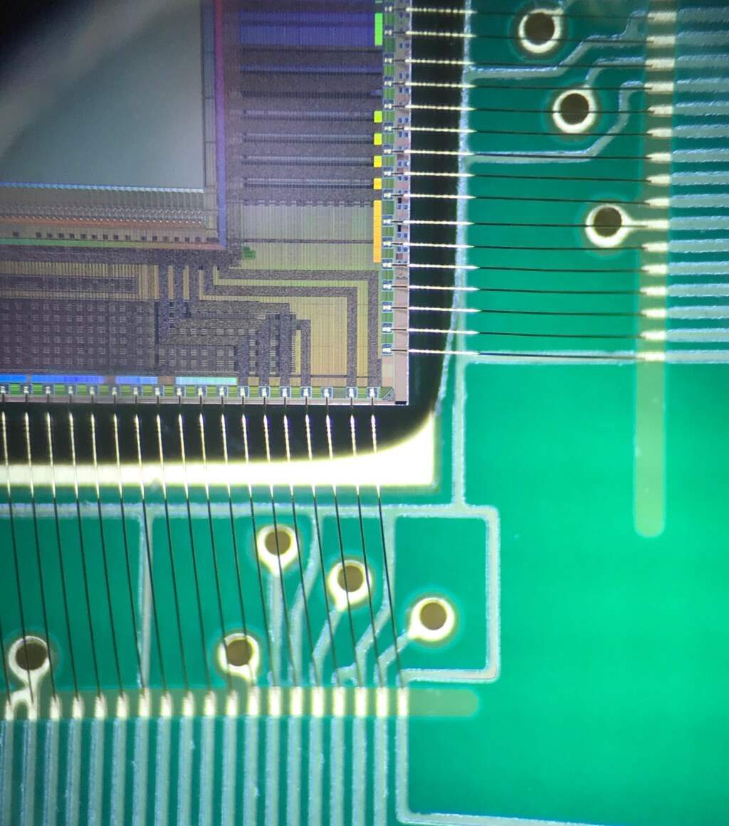
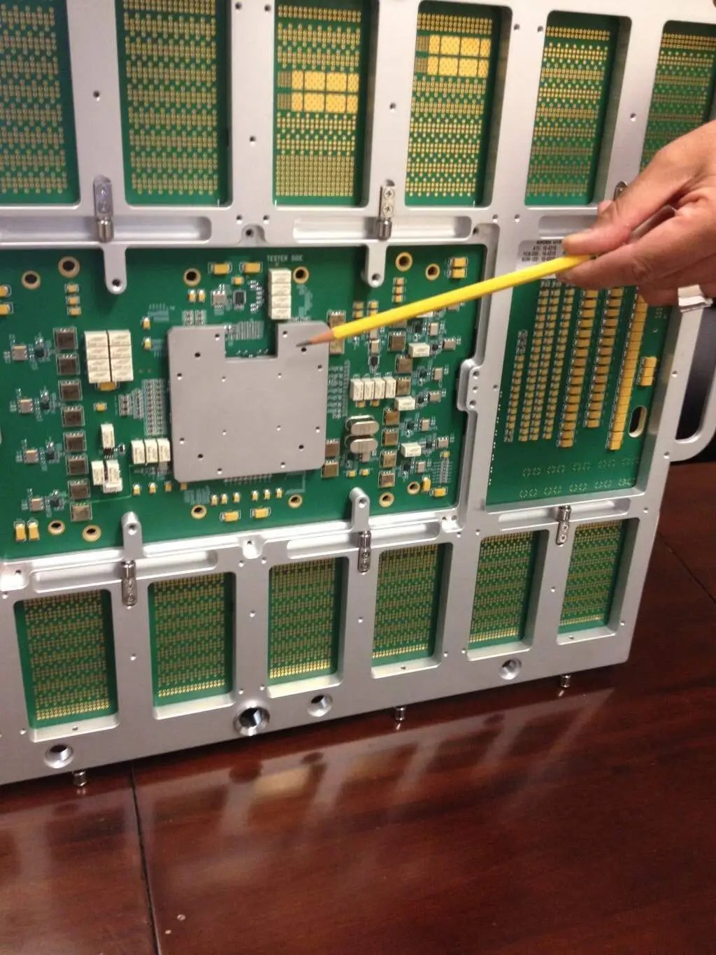
Custom Solutions from Wafer Probe to Final Test
Dynamic Test Solutions Case Study
ATE PCBs Demand Quick Turn and High Quality
Published in EE Web

Unleashing Quantum Potential
Published on SMTnet

Delivering Custom RF Amplifiers
Broadband Wireless Case Study
Improving Health Through Nutrition Insight
Opsis Health Case Study

Space-Qualified Electronics Manufacturing
Published in Global SMT & Packaging
International Traffic In Arms Regulation (ITAR)
Naprotek - 90 Rose Orchard Way

International Traffic In Arms Regulation (ITAR)
Naprotek - 2085 Zanker Road

Quality Management Systems
ISO 9001:2015 - 90 Rose Orchard Way
.png?width=1500&height=1200&name=ISO%209001%20Mark%20(1).png)
Quality Management Systems
ISO 9001:2015 - 2085 Zanker Road
QMS — Aviation, Space, and Defense
AS9100D - 90 Rose Orchard Way
.png?width=1500&height=1200&name=AS9100D%20and%20ISO%209001%20Mark%20(1).png)
QMS — Aviation, Space, and Defense
AS9100D - 2085 Zanker Road
QMS — Medical Devices
ISO 13485:2016 - 90 Rose Orchard Way
.png?width=1500&height=1200&name=ISO%2013485%20Mark%20(1).png)
QMS — Medical Devices
ISO 13485:2016 - 2085 Zanker Road
Quality at Naprotek
Conflict Minerals Statement

CMRT 6.4 Conflict Minerals Report
90 Rose Orchard Way
CMRT 6.4 Conflict Minerals Report
2085 Zanker Road
Quality at Naprotek
RoHS Compliance Statement
Quality at Naprotek
REACH Compliance Statement
Quality at Naprotek
Prop 65 Compliance Statement
Quality at Naprotek
Terms & Conditions of Purchase
Quality at Naprotek
Terms & Conditions of Sale
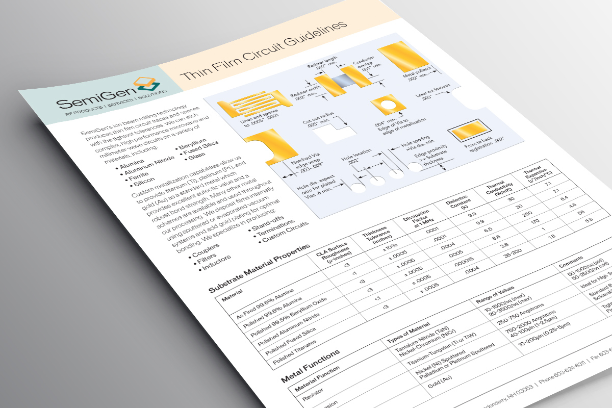
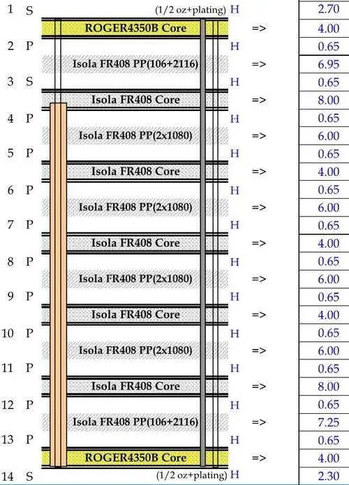
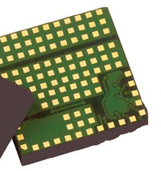
Thin Film Circuit Design Guidelines
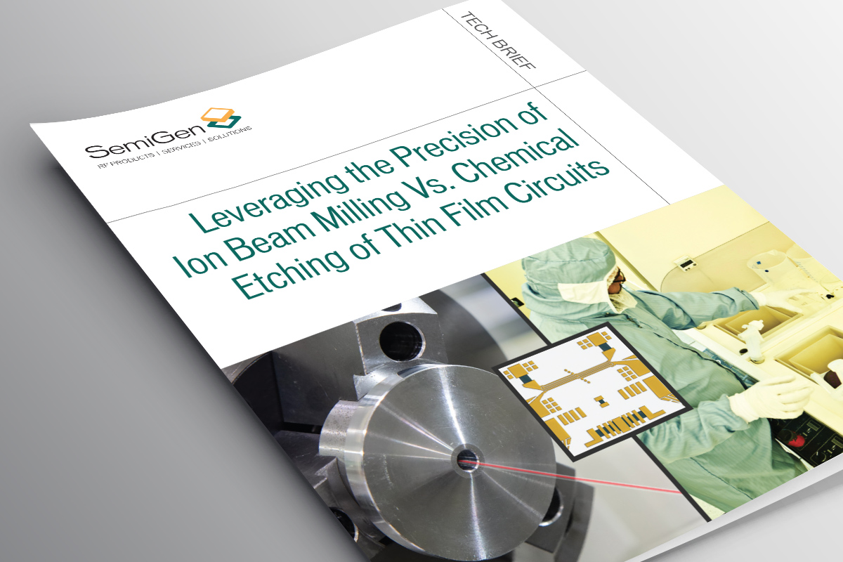
Leveraging the Precision of Ion Beam Milling Vs. Chemical Etching of Thin Film Circuits
Tech Brief
Eutectic Die-Attach of GaN and GaAs MMICs
Tech Brief

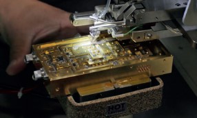
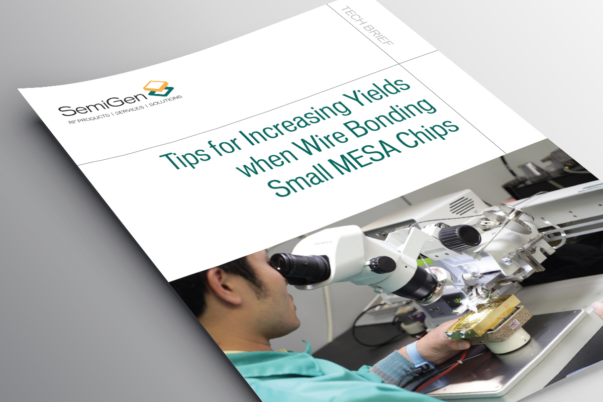
Tips for Increasing Yields when Wire Bonding Small MESA Chips
Tech Brief
How RF and Microwave Companies Can be Empowered by US-based Contract Manufacturing
Tech Brief

PCB Microelectronics Assembly Takes Center Stage for Medical Miniaturization
Published in Medical Design Briefs
PCBs on the Medical Ventilator Frontlines
Published in EE Web
3 key steps for IoT PCB SMT and microelectronics assembly
Published by IoT Agenda

Understand the basics of multi-tier wire bonding
Published by IoT Agenda
Epoxy’s role in IoT device PCB assembly and manufacturing
Published by IoT Agenda
Protect IoT bare dies and wire bonds for high reliability
Published by IoT Agenda
IoT PCB microelectronics manufacturing calls for intricate tools
Published by IoT Agenda
PCB Microelectronics Tools for Intricate Inspection and Calibration
Published in EE Web
Die Attach Comes to PCBs
Published in EE Web
Get linked up with anisotropic conductive film for your IoT devices
Published by IoT Agenda
Revisiting ISO 13485 For Wire Bonding Quality and Reliability
Published in EE Web
Failures in IoT PCB wire bond loops
Published by IoT Agenda
Ensure IoT device reliability via die shear strength testing
Published by IoT Agenda
Pinpoint IoT PCB wire bonding reliability
Published by IoT Agenda
Get your wires straight for IoT
Published by IoT Agenda
PADS accelerates IoT PCB design
Published by IoT Agenda
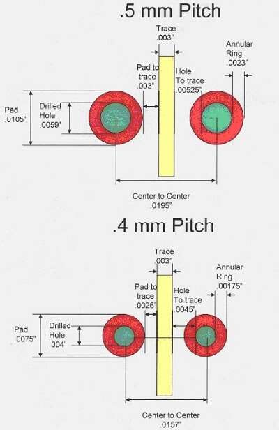
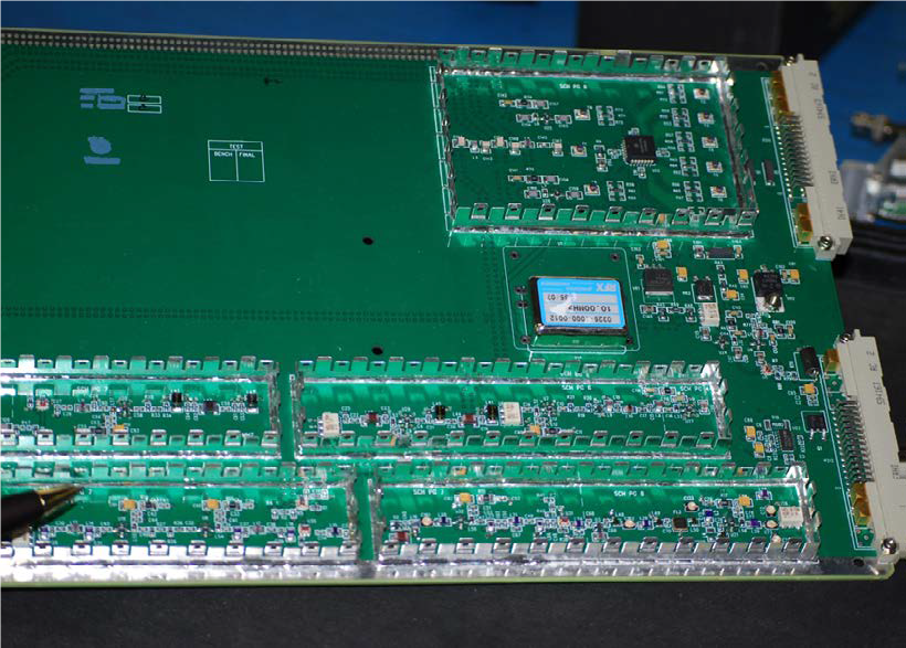
Key Design Steps for DUT Areas on ATE PCBs
Published in EE Web
Anatomy of next-gen IoT PCBs
Published by IoT Agenda
A careful look at RF for your IoT PCBs
Published by IoT Agenda
Anatomy of ATE PCB Assembly
Published in EE Times

Flex Circuit Design Primer for Wearable/IoT Device
Published in EE Times
Wearable PCB Designs Require Attention to Fundamentals
Published in EE Times
7 Tips for Overcoming PCB Electromagnetic Issues
Published in EE Times

DOEs Rescue Questionable Medical Electronics PCBs
Published in Medical Design Briefs
Avoiding embedded PCB design defects
Published in Embedded

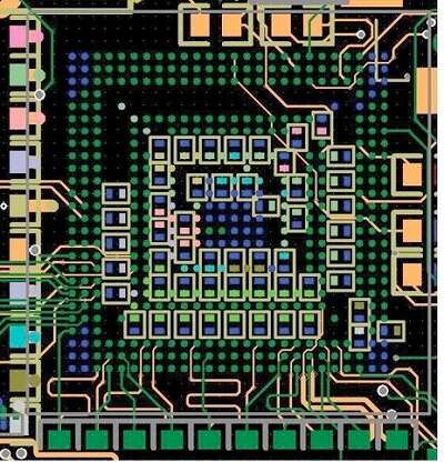
Making efficient use of BGA signal routing in PCB designs
Published in Embedded

Bringing experimental development methods to PCB design and manufacturing
Published in Embedded
Characteristics of a Third-Level PCB Assembly
Published in Printed Circuit Design & Fab
Overlooking design-for-test can lead to costly PCB design rework
Published in Embedded
PCB Design and Assembly for Medical Electronic OEMs
Published in EE Web
Tighter Scrutiny Needed for PCB Cleaning Agents
Published in SMT007
Applying Design for Manufacturing (DFM) to PCB development
Published in Embedded
Uncovering Assembly Problems of High-Speed PCBs
Published in SMT007

The Basics of Thermal Profiling for Sensitive Components
Published in Circuits Assembly
Migrating your embedded PCB design from DDR2/3 to DDR4 SDRAMs
Published in Embedded

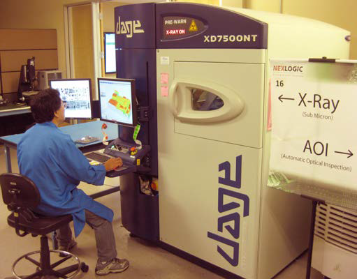
Yardsticks for Gauging AOI Effectiveness
Published in Circuits Assembly
EMS Discovers Mature IC Technologies
Published in SMT Magazine
Design Practices for Panelization and Depanelization
Published in Printed Circuit Design & Fab
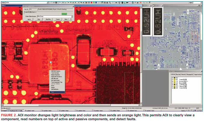
Get Another Look Into AOI
Published in SMT Magazine
Seven ways to avoid embedded PCB engineering change orders
Published in Embedded
Using Forensics to Improve PCB Design and Assembly
Published in Printed Circuit Design & Fab
Saving your embedded printed circuit board design with forensic technology
Published in Embedded
Critical guidelines for RF and microwave PCB Design
Published in Embedded
High-Reliability PCBs in Mil/Aero Applications
Published in The PCB Magazine
FAI: An Ounce of Prevention, Worth a Pound of Cure
Published in SMT Magazine
The Intricacies of RF Design and Assembly
Published in SMT Magazine
Building quality & signal integrity into PoP-based PCB design & assembly
Published in Embedded
Building quality & signal integrity into PoP-based PCB design & assembly
Published in Embedded